


The Itanium family of processors has characteristics that are different from the RISC chips presented elsewhere in this section. A block diagram of the Itanium 2 is shown in 12.
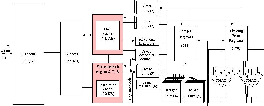
Figure 12: Block diagram of the Intel Itanium 2.
We show here the fastest version that also harbours the largest L3 cache of 9
MB. Figure 12
shows a large amount of functional units that must be kept busy. This
is done by large instruction words of 128 bits that contain 3 41-bit
instructions and a 5-bit template that aids in steering and decoding
the instructions. This is an idea that is inherited from the Very Large
Instruction Word (VLIW) machines that have been on the market for some
time about ten years ago. The two load/store units fetch two
instruction words per cycle so six instructions per cycle are
dispatched. The Itanium has also in common with these systems that the
scheduling of instructions, unlike in RISC processors, is not done
dynamically at run time but rather by the compiler. The VLIW-like
operation is enhanced with predicated execution which makes it possible
to execute instructions in parallel that normally would have to wait
for the result of a branch test. Intel calls this refreshed VLIW mode
of operation EPIC, Explicit Parallel Instruction Computing.
Furthermore, load instructions can be moved and the loaded variable
used before a branch or a store by replacing this piece of code by a
test on the place is originally came from to see whether the operations
have been valid. To keep track of the advanced loads an Advanced Load
Address Table records them. When a check is made about the validness of
an operation depending on the advanced load, the ALAT is searched and
when no entry is present the operation chain leading to the check is
invalidated and the appropriate fix-up code is executed. Note that
this is code that is generated at compile time so no control
speculation hardware is needed for this kind of speculative execution.
This would become exceedingly complex for the many functional units
that may be simultaneously in operation at any time.
As can be seen from Figure 12 there are four
floating-point units capable of performing Fused Multiply Accumulate
(FMAC) operations. However, two of these work at the full 82-bit
precision which is the internal standard on Itanium processors, while
the other two can only be used for 32-bit precision operations. When
working in the customary 64-bit precision the Itanium has a theoretical
peak performance of 4 Gflop/s at a clock frequency of 1 GHz. Using
32-bit floating arithmetic, the peak is doubled.
In the first generation Itanium there were 4 integer units for integer
arithmetic and other integer or character manipulations. Because the
integer performance of this processor was modest, 2 integer units have
been added to improve this. In addition four MMX units to accommodate
instructions for multi-media operations, an inheritance from the Intel
Pentium processor family. For compatibility with this Pentium family a
special IA-32 decode and control unit is present.
The register files for integers and floating-point numbers is large:
128 each. However, only the first 32 entries of these registers are
fixed while entries 33--128 are implemented as a register stack. The
primary data and instruction caches are 4-way set associative and
rather small: 16 KB each. This is the same as in the former Itanium
processor. However, speed of the L1 cache is now doubled to full
speed: data and instructions can now be delivered every clock cycle to
the registers. Further more the secondary cache has been enlarged from
96 KB to 256 KB and it is 8-way set-associative. Moreover, the L3 cache
is moved onto the chip and is no less than up to 9 MB. This cache structure
greatly improves the bandwidth to the processor core, on average by a factor of
3. This does even more for the performance improvement than the increase in
clock speed from 800 MHz to 1.6 GHz. Also the bandwidth from/to memory has
increased by more than a factor of 3. The bus is now 128 bits wide and operates
at a clock frequency of 400 MHz, totaling to 6.4 GB/s in comparison to 2.1 GB/s
for its predecessor. As the frontside bus will not be enlarged, this speed will
not scale with upcoming increases of the processor speed and so again may
frustrate overall speedup in the near future.
The introduction of the first Itanium has been deferred time and again which
quenched the interest for use in high-performance systems. With the
availability of the Itanium 2 in the second half of 2002 the adoption has sped
up. Apart from HP/Compaq also Bull, Fujitsu, NEC, SGI and Unisys are offering
now multiprocessor systems with this processor and the Alpha, PA-RISC, SPARC,
and MIPS processors as employed by HP/Compaq, Fujitsu, and SGI respectively
will be phased out in the next few years.